
GPU Architecture Explained
You have probably heard that GPUs are fast. You may have heard phrases like "massively parallel" or "thousands of cores." But what does any of that actually mean, and why does it matter for writing fast code?
This article walks through GPU architecture from scratch using NVIDIA's H100 as the reference, because the H100 is the chip that powers most serious AI training today. Every concept here applies to older GPUs too, just with smaller numbers.
Why GPUs exist at all
A CPU is a general-purpose processor. It is built to run one stream of instructions as fast as possible, doing things like branching into different code paths, predicting what comes next, and caching data for unpredictable access patterns. A modern Intel or AMD desktop core runs at around 5 GHz and has hardware that guesses the future to avoid waiting.
A GPU is the opposite trade-off. It gives up most of that complexity and uses the freed-up silicon for raw compute units instead. The result is a chip that can do many simple arithmetic operations in parallel but struggles with code that jumps around unpredictably.
This matters because neural networks, graphics rendering, and scientific simulation all share one trait: the same arithmetic applied to millions of independent values. A matrix multiply is the same dot product, repeated millions of times. That shape fits parallel hardware perfectly.
The big picture: how a GPU is organized
A GPU die is not just a flat pile of cores. It is organized into a strict hierarchy. Understanding that hierarchy is the key to understanding GPU performance.
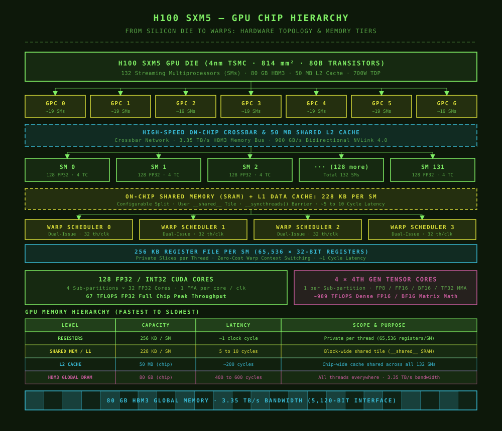
Start at the top.
The whole chip is called the die. The H100 SXM5 die contains 132 Streaming Multiprocessors, 80 GB of HBM3 memory, and a 50 MB L2 cache shared across the whole chip.
Below the die, the hardware is grouped into GPCs (Graphics Processing Clusters). The H100 has 7 of them. A GPC is mostly a grouping concept, useful for thinking about how NVIDIA routes data around the chip. For most CUDA programming you will never think about GPCs directly.
Inside each GPC are the SMs (Streaming Multiprocessors). This is where the real work happens. The SM is the fundamental compute unit of a GPU, roughly analogous to a CPU core. Everything else on the chip exists to feed the SMs with data and instructions.
Cutting across everything is the memory system. The H100 connects its SMs to 80 GB of HBM3 (High Bandwidth Memory) via an on-chip interconnect, delivering 3.35 TB/s of bandwidth. For comparison, a top-of-the-line CPU memory controller might manage 100 to 200 GB/s. That bandwidth gap is a big part of why GPUs are so effective for data-intensive workloads.
What lives inside one SM
Every SM is a self-contained little processor. Zoom into one and you find:
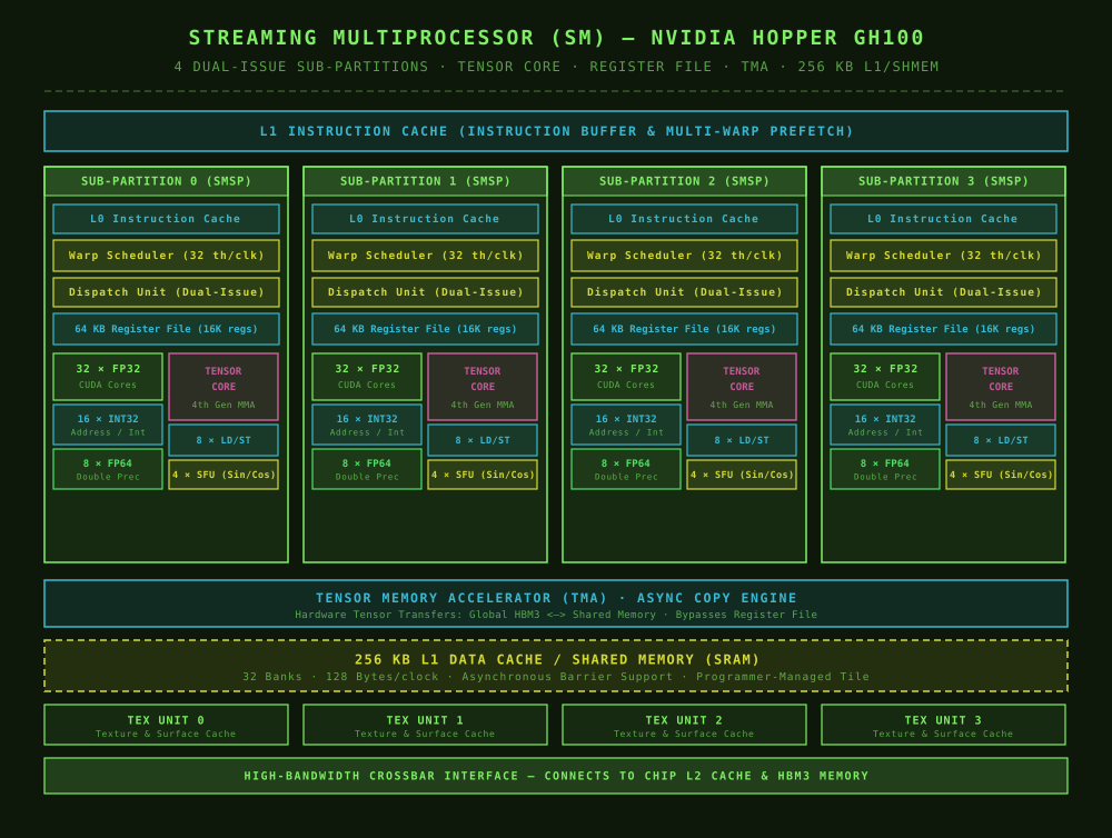
Let's walk through each piece.
Warp schedulers
An SM on the H100 has 4 warp schedulers. Each scheduler is responsible for keeping a pool of warps ready to execute. A warp is a group of 32 threads that all run the same instruction simultaneously.
Here is why this matters. Loading data from global memory takes 400 to 600 clock cycles. Rather than stall the whole SM while waiting, the warp scheduler simply picks a different warp from its ready queue and runs that instead. By the time the original warp's data arrives, dozens of other warps have made progress. This technique is called latency hiding, and it is the GPU's primary way of tolerating slow memory access.
With 4 schedulers each managing up to 16 warps, a single SM can juggle up to 64 warps (2,048 threads) at once. Most of those warps are waiting on memory at any given moment. The handful that are ready keep the arithmetic units busy.
The register file
Each SM has a 256 KB register file, containing 65,536 individual 32-bit registers. That sounds like a lot, but it is shared across all the threads running concurrently on the SM.
Each thread gets a private slice of this register file. The key insight is that switching from one warp to another costs nothing: the warp scheduler just starts reading from a different slice of the register file. There is no "context save" like you get on a CPU. This zero-cost switching is what makes the latency-hiding trick work at full speed.
More registers per thread means you can keep more intermediate values on-chip (faster), but it also means fewer threads can fit on the SM at once (lower occupancy). Compiler flags like --maxrregcount let you tune this trade-off.
CUDA Cores (FP32)
The H100 SM has 128 FP32 CUDA Cores, split across 4 partitions of 32. Each core does one floating-point multiply-add per clock cycle. With the H100 running at around 1.83 GHz, that works out to about 67 TFLOPS of FP32 throughput across the full chip.
CUDA Cores are what execute your ordinary float arithmetic, basic integer math, and comparisons. For a long time these were the only compute units GPUs had.
Tensor Cores
The H100 SM also has 4 fourth-generation Tensor Cores. These are a different beast entirely.
A Tensor Core does not compute one multiply-add per cycle. It computes an entire small matrix multiply-accumulate (MMA) operation in one instruction. On the H100, one Tensor Core instruction operating on FP16 data produces 256 multiply-add operations per cycle. Across the full chip, that gives you around 989 TFLOPS of FP16 throughput with sparsity, or roughly 495 TFLOPS dense.
To put that in perspective: the FP32 CUDA Cores give you 67 TFLOPS. The Tensor Cores give you roughly 7x more throughput, but only for the specific shapes of matrix arithmetic they are designed for.
This is why modern deep learning frameworks like PyTorch try very hard to express operations as matrix multiplications and why they push FP16 or BF16 precision wherever possible. Falling off the Tensor Core path is one of the most common reasons a kernel runs slower than expected.
Shared memory and L1 cache
Every SM has a pool of on-chip SRAM that serves double duty as a configurable split between L1 data cache and user-controlled shared memory. On the H100 that pool is 228 KB per SM.
The L1 side is hardware-managed: the GPU automatically caches global memory reads here, and you do not control it directly.
The shared memory side is programmer-controlled. When you declare __shared__ float tile[32][32]; in a CUDA kernel, you are carving out space in this pool. Shared memory is accessible by every thread in the same thread block, and it runs at roughly the same speed as registers (a few cycles of latency) rather than the hundreds of cycles needed for global memory.
This is the core of the tiled matrix multiplication pattern: load a tile of the input matrices from slow global memory into fast shared memory once, compute against it many times, then move to the next tile. The shared memory acts as a software-managed cache.
How your kernel maps onto this hardware
When you launch a CUDA kernel, you specify a grid of thread blocks. The GPU's work distributor assigns each thread block to one SM. Once assigned, a block stays on that SM until it finishes.
The SM splits each thread block into warps of 32 threads (consecutive thread IDs, so threads 0 to 31 are warp 0, threads 32 to 63 are warp 1, and so on). All the warps from all the blocks resident on an SM share the warp schedulers.
A concrete example with the H100: you launch a kernel with 256-thread blocks.
- Each block becomes 8 warps (256 / 32).
- The H100 can hold up to 32 thread blocks per SM and up to 64 warps per SM.
- With 256-thread blocks, you can fit 8 blocks x 8 warps = 64 warps, which exactly saturates the SM.
- Multiply by 132 SMs: the whole chip can run about 16,000 warps at once, covering more than 500,000 threads.
None of those threads are running at exactly the same moment. At any cycle, each of the 4 schedulers picks one ready warp and issues one instruction. The other warps are either waiting on memory or waiting for their turn. The magic is that switching between them is instantaneous.
The memory hierarchy, from fast to slow
One more thing beginners often find confusing is the layered memory system. Here is the full stack from fastest to slowest:
| Level | Size (H100 SM) | Latency | Who can access it |
|---|---|---|---|
| Registers | 256 KB / SM | ~1 cycle | One thread only |
| Shared memory | Up to 228 KB / SM | ~5 to 10 cycles | All threads in one block |
| L1 cache | Shares the 228 KB pool | ~30 cycles | All threads in one SM (automatic) |
| L2 cache | 50 MB (whole chip) | ~200 cycles | All threads on the chip |
| HBM3 (global memory) | 80 GB | ~400 to 600 cycles | All threads everywhere |
The pattern is simple: the closer memory is to the compute units, the faster and smaller it is. Writing a fast kernel almost always means arranging your algorithm to spend most of its time in registers and shared memory, and to visit global memory as rarely as possible.
A real example: why matrix multiply is so fast on GPUs
Suppose you multiply two 4096 x 4096 float32 matrices. That requires about 137 billion floating-point operations. On a CPU core running at 5 GHz with 16-wide SIMD, you get around 160 GFLOPS. That calculation would take roughly 860 ms.
On an H100 with cuBLAS using Tensor Cores in FP16: roughly 1.3 ms. That is a 660x difference.
Why? Three reasons:
- Parallelism. The H100 has 132 SMs x 4 Tensor Cores x 256 operations per cycle, all running at once.
- Data reuse through tiling. Shared memory means each value loaded from HBM3 contributes to many multiply-add operations before it is discarded. The arithmetic intensity climbs high enough to stay off the memory bandwidth limit.
- Precision. Using FP16 instead of FP32 halves the data movement and doubles the throughput on Tensor Cores.
Everything in high-performance GPU programming, from attention kernels to convolution to custom operator fusion, is essentially an attempt to achieve the same three properties for whatever operation you care about.
What Hopper changed (and what Blackwell is doing next)
The H100 introduced a few architectural ideas worth knowing, because they show where GPU design is heading.
The Transformer Engine is a hardware block dedicated to automatically selecting the right floating-point precision per layer during training. It tracks scaling factors and switches between FP8 and BF16 dynamically, keeping Tensor Core utilization high without requiring you to manually tune precision.
Asynchronous memory copy (TMA, Tensor Memory Accelerator) lets the hardware fetch data from global memory into shared memory independently of the warp schedulers. Previously, loading data into shared memory required warp instructions, which consumed scheduler capacity. With TMA, a kernel can dedicate some warps to compute and let the hardware pipeline the data loading in the background.
NVLink 4.0 and NVSwitch connect multiple H100 GPUs with 900 GB/s of bidirectional bandwidth per GPU. This matters for model parallelism: moving tensor shards between GPUs over NVLink is fast enough that it no longer dominates training time for most models.
The Blackwell generation (B100, B200, announced 2024) takes these further with FP4 Tensor Core support, a second-generation Transformer Engine, and a new die-to-die interconnect that tiles two Blackwell dies into one logical GPU with 10 TB/s of internal bandwidth. The H100 concepts still apply; Blackwell just adds more levels to the hierarchy.
What to take away
A GPU is not a magic fast box. It is a specific piece of hardware with a specific hierarchy: GPCs containing SMs, each SM containing warp schedulers, CUDA Cores, Tensor Cores, a register file, and shared memory, all backed by high-bandwidth HBM.
Your code runs fast when it matches that hierarchy:
- Threads that do independent work with no communication are cheap to parallelize.
- Data that lives in registers and shared memory moves fast.
- Data that lives in global HBM moves slow, so use tiling to amortize each load across many operations.
- Operations expressible as matrix multiplications can use Tensor Cores and run at 7x the throughput of scalar FP32.
Everything else in GPU programming is either filling in the details of these principles or working around specific hardware limits.
Keep reading
- What is a Streaming Multiprocessor? goes deeper on SM internals
- What is a Warp? explains how 32 threads become one scheduling unit
- Tiled GEMM is a hands-on walkthrough of shared memory tiling
- NVIDIA H100 Tensor Core GPU Architecture (NVIDIA whitepaper)
- Hopper Architecture In-Depth (NVIDIA Developer Blog)
- Dissecting the Ampere GPU Architecture for contrast with the previous generation
About the author
Ritesh Yadav works as an AI/ML Engineer. He writes independent research notes on ML performance, infrastructure, and systems, covering CUDA, low-latency inference, generative AI, distributed training, Kubernetes, and LLMOps.